Recently, a significant advancement in the study of carrier dynamics in wide-bandgap nitrides has been made by Professor Suhuai Wei, Chair Professor and Dean of the School of Physics at the Eastern Institute of Technology, Ningbo, in collaboration with the team of Researchers Zhiming Shi, Xiaojuan Sun, and Dabing Li from the Changchun Institute of Optics, Fine Mechanics and Physics (CIOMP) of the Chinese Academy of Sciences. They proposed a novel strategy utilizing interface defect engineering to accelerate electron cooling, effectively addressing the long-standing issue of asymmetric carrier injection that plagues the efficiency of nitride-based ultraviolet light-emitting diodes. This work, entitled "Overcoming asymmetric carrier injection in III-nitride light-emitting diodes through defect engineering", was published in the prestigious physics journal Physical Review Letters on July 8, 2025.
First-Principles Calculations Reveal the Physical Mechanism of Defect-Accelerated Electron Cooling
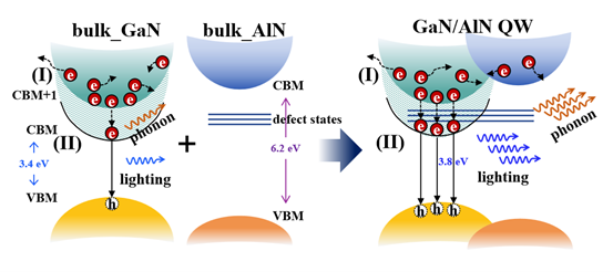
AlGaN-based UV LEDs are core components for next-generation applications like high-density optical storage, sterilization, and air purification. A key factor limiting their efficiency is the asymmetry in cooling rates between electrons and holes: the energy relaxation process for electrons is significantly slower than for holes, leading to low radiative recombination efficiency. Conventional approaches often employ electron blocking layers (EBLs) to improve electron injection efficiency, but these face challenges such as complex design, introduction of additional potential barriers, and material incompatibility, making it difficult to fundamentally optimize carrier dynamics.
Based on their analysis of nitride band structures and carrier dynamics, the team led by Professor Suhuai Wei and researchers Zhiming Shi, Xiaojuan Sun, and Dabing Li pioneered the idea of enhancing the electron cooling rate by intentionally introducing and controlling nitrogen vacancy defects at the GaN/AlN quantum well interface. These defect states act as intermediate energy levels, significantly strengthening electron-phonon interactions and thereby accelerating electron cooling towards the conduction band minimum. First-principles calculations demonstrate that this strategy can shorten the electron cooling time by over an order of magnitude, effectively achieving a dynamic balance with the hole cooling rate and substantially boosting the luminescence efficiency. Compared to traditional EBL structures, this method enables precise control of electron dynamics without the need for complex additional layer design. This research also expands the boundaries of semiconductor defect physics, systematically validating the "beneficial" role defects can play in tuning device performance, challenging the conventional view of defects as purely detrimental. It provides crucial theoretical support and new design principles for defect engineering in next-generation electronic and optoelectronic devices.
These findings deepen the understanding of the interaction mechanism between carrier dynamics and defects in wide-bandgap nitrides and are of great significance for enhancing the internal quantum efficiency of UV LEDs and realizing high-performance optoelectronic devices.
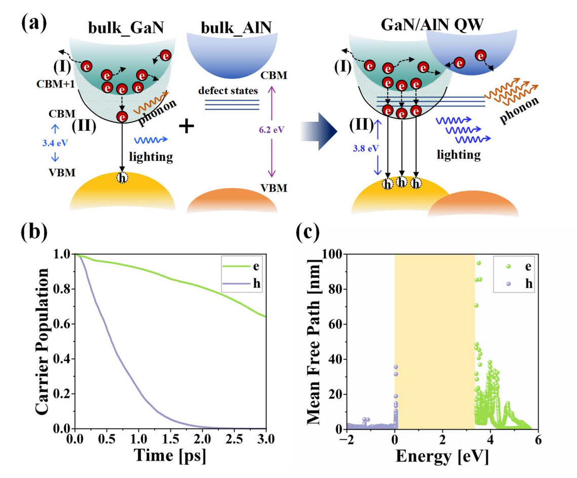
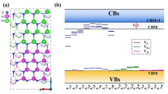
Figure 2. Spatial distribution of point defects within the quantum well and the corresponding energy distribution of the defect states.
The first author of the paper is Yuxin Yang,a Ph.D student from CIOMP, Chinese Academy of Sciences. The corresponding authors are Researcher Zhiming Shi, Professor Suhuai Wei, Researcher Xiaojuan Sun, and Researcher Dabing Li.